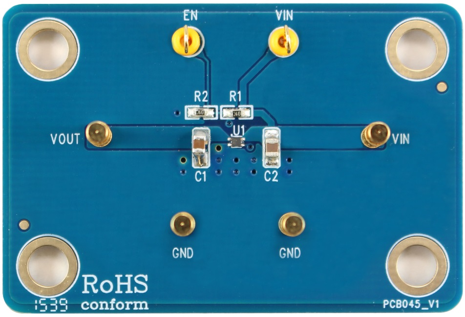
Purpose
The RT9073A is a low-dropout (LDO) voltage regulators with enable function that operates from 1.2V to 5.5V. It provides up to 250mA of output current and offers low-power operation in miniaturized packaging.
The features of low quiescent current as low as 1µA and almost zero disable current is ideal for powering the battery equipment to a longer service life. The RT9073A is stable with the ceramic output capacitor over its wide input range from 1.2V to 5.5V and the entire range of output load current (0mA to 250mA).
Introduction
General Product Information
The RT9073A is a low quiescent current linear regulator designed especially for low external components system. The input voltage range is from 1.2V to 5.5V. The RT9073A builds in a P-MOSFET output transistor which provides a low switch-on resistance for low dropout voltage applications.
The Error Amplifier compares the internal reference voltage with the output feedback voltage from the internal divider, and controls the Gate voltage of P-MOSFET to support good line regulation and load regulation at output voltage.
Product Feature
-
1µA Ground Current at no Load
-
PSRR = 75dB at 1kHz
-
Adjustable Output Voltage Available by Specific Application
-
±2% Output Accuracy
-
250mA (VIN ≥ 2.3V) Output Current with EN
-
Low (0.1µA) Disable Current
-
1.2V to 5.5V Operating Input Voltage
-
Dropout Voltage : 0.5V at 250mA when VOUT ≥ 3V
-
Support Fixed Output Voltage 3.3V
-
Stable with Ceramic or Tantalum Capacitor
-
Current Limit Protection
-
Over Temperature Protection
-
ZQFN-4L 1x1 Packages Available
Key Performance Summary Table
|
Key Features
|
Evaluation Board Number : PCB045_V1
|
|
Input Voltage Range
|
1.2V to 5.5V
|
|
Output Current Limit
|
350mA
|
|
Power Supply Rejection Ratio
|
75dB
|
|
Default Marking & Package Type
|
RT9073A-33GQZ, ZQFN-4L 1x1
|
|
VCC Consumption Current
|
1µA
|
Bench Test Setup Conditions
Headers Description and Placement

Please carefully inspect the EVB IC and external components, comparing them to the following Bill of Materials, to ensure that all components are installed and undamaged. If any components are missing or damaged during transportation, please contact the distributor or send e-mail to evb_service@richtek.com
Test Points
The EVB is provided with the test points and pin names listed in the table below.
|
Test point/
Pin name
|
Signal
|
Comment (expected waveforms or voltage levels on test points)
|
|
VOUT
|
Output voltage
|
Default output voltage = 3.3V.
|
|
GND
|
Ground
|
Ground.
|
|
EN
|
Enable
|
Enable Control Input.
|
|
VIN
|
Input voltage
|
Input voltage range = 1.2V to 5.5V.
|
Power-up & Measurement Procedure
1. Connect input power (1.2V < VIN < 5.5V) to VIN test pin.
2. VIN/VOUT placed 1µF capacitor.
3. Observe the output voltage is correct.
Schematic, Bill of Materials & Board Layout
EVB Schematic Diagram

Bill of Materials
|
Reference
|
Qty
|
Part Number
|
Description
|
Package
|
Manufacture
|
|
U1
|
1
|
RT9073A-33GQZ
|
Single Output LDO
|
ZQFN-4L 1x1
|
Richtek
|
|
C1, C2
|
2
|
C2012X7R1E105KT00HN
|
1µF/25V
|
C-0805
|
TDK
|
|
GP1
|
1
|
|
VOUT
|
SIP-1P-GP
|
|
|
GP2
|
1
|
|
VIN
|
SIP-1P-GP
|
|
|
GP3, GP4
|
2
|
|
GND
|
SIP-1P-GP
|
|
|
R1, R2
|
2
|
WR06X1002F
|
10k
|
R-0603
|
WALSIN
|
|
TP1
|
1
|
|
IN
|
SIP-1P-TP
|
|
|
TP2
|
1
|
|
EN
|
SIP-1P-TP
|
|
|
Z1, Z2, Z3, Z4
|
4
|
|
SIP-1P-M
|
SIP-1P-M
|
|
|
Z5, Z6
|
2
|
|
FK_1
|
FK_1
|
|
PCB Layout

Top View

Bottom View